

 Product
 Brand
Brand Articles
 Tools
Tools
The Practical Engineer’s Guide to the NE555N Timer: Pinout, Setup, and Troubleshooting
Hardware timers provide deterministic pulse generation without the overhead of software execution. The NE555N timer is a precision bipolar integrated circuit housed in a Plastic DIP-8 package, designed to generate accurate time delays or oscillation. Operating between 4.5V and 16V with a 200mA sink/source capacity, it remains a foundational component for electronics engineers, repair technicians, and component sourcing teams.
This guide details the NE555N pinout, core datasheet specifications, mathematical setup for its primary modes, and real-world troubleshooting to prevent common breadboard failures. For a broader overview of the IC family's history, refer to this overview of the 555 Timer.
NE555N Pinout and Internal Architecture
The NE555N features an 8-pin layout comprising Ground, Trigger, Output, Reset, Control Voltage, Threshold, Discharge, and Vcc, which interface directly with internal comparators and a flip-flop.
The 8-Pin DIP Layout
Understanding the physical pinout is required for accurate breadboard prototyping. The pins are numbered counterclockwise starting from the top left (indicated by a notch or dot on the package):
Ground (GND): Connects to the negative rail of the power supply.
Trigger: Monitors the timing capacitor's voltage. A voltage drop below 1/3 Vcc initiates the timing cycle.
Output: Delivers the resulting square wave or pulse. It can source or sink current.
Reset: Interrupts the timing cycle when driven low.
Control Voltage: Allows external adjustment of the internal threshold voltages.
Threshold: Monitors the timing capacitor's voltage. A voltage rise above 2/3 Vcc ends the timing cycle.
Discharge: Provides a path to ground to discharge the external timing capacitor.
Vcc: Connects to the positive power supply rail.
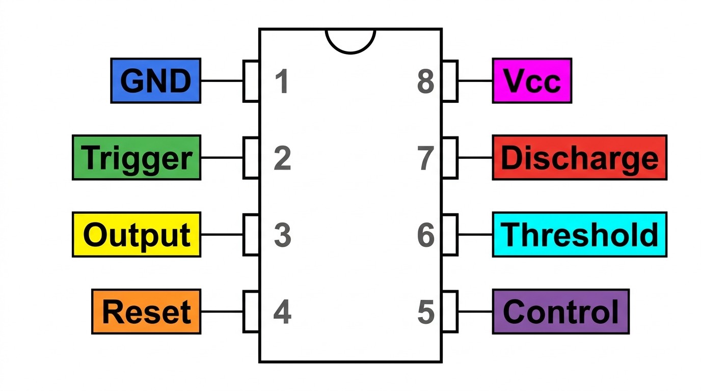
Internal Architecture and Name Origin
The internal architecture consists of two voltage comparators, a bistable flip-flop, a discharge transistor, and a resistor divider network. In visual stress tests and schematic breakdowns, experts point out the literal origin of the component's designation. As noted in recent video intelligence analyzing the internal schematic: "The name of the IC derives from the three 5 kilohm resistors you can see on the front."
These three 5kΩ resistors are configured as a voltage divider between Vcc and Ground. Consequently, they establish the strict reference voltages for the internal comparators: exactly 1/3 Vcc for the Trigger and 2/3 Vcc for the Threshold.
📺 Introduction to 555 Timers | Basic Circuits
NE555N Datasheet Specifications and Variants
The NE555N operates safely between 4.5V and 15V, with an absolute maximum rating of 18V, and can sink or source up to 200mA of current.
Core Operating Limits
According to Texas Instruments and STMicroelectronics datasheets, the NE555N has a recommended operating voltage of 4.5V to 15V (up to 16V for some manufacturers). The absolute maximum voltage rating is 18V. Exceeding 18V will permanently damage the silicon.
Furthermore, the IC features a maximum output current capacity (sink and source) of 200mA, with 225mA listed as the absolute maximum stress limit.
Scenario Application: With a 200mA capacity, the NE555N can drive standard LEDs or small electromechanical relays directly from Pin 3. However, for users attempting to drive a 500mA DC motor, the NE555N will overheat and fail. In that scenario, the output pin must trigger an external N-channel MOSFET to handle the higher load.
Suffix Decoding: NE555N vs. NE555P vs. ICM7555
Component sourcing teams frequently encounter confusion regarding part suffixes. The "NE" prefix specifies a commercial operating temperature range of 0°C to 70°C. The "N" suffix (historically used by Signetics/Philips, now STMicroelectronics/ON Semi) and the "P" suffix (used by Texas Instruments) both designate an 8-pin Plastic Dual In-Line Package (PDIP-8). Therefore, an NE555N and an NE555P are functionally identical and interchangeable.
Conversely, the ICM7555 and TLC555 are CMOS variants. While the bipolar NE555N draws 3-10mA of quiescent current, CMOS variants draw approximately 80µA and can operate down to 2V.
NE555N Variant Matrix
| Specification | NE555N / NE555P (Bipolar) | ICM7555 / TLC555 (CMOS) |
|---|---|---|
| Operating Voltage | 4.5V to 16V | 2.0V to 18V |
| Quiescent Current | 3mA to 10mA | ~80µA |
| Max Output Current | 200mA (Sink/Source) | 10mA to 100mA (Varies) |
| Primary Use Case | Driving relays, high-current loads | Battery-powered circuits, logic levels |
Core Operating Modes and Circuit Setup
The NE555N operates in three primary modes: Astable for continuous oscillation, Monostable for single-pulse generation, and Bistable as a basic memory cell.
Astable Mode (Oscillator)
In Astable mode, the NE555N generates a continuous square wave. The timing is dictated by two resistors (R1 and R2) and one capacitor (C).
The standard formulas are:
Time High (Thigh): 0.693 × (R1 + R2) × C
Time Low (Tlow): 0.693 × R2 × C
Frequency (f): 1.44 / ((R1 + 2R2) × C)
The constants in these formulas are derived directly from the internal voltage divider thresholds. The 0.693 multiplier is derived from ln(2), representing the time it takes an RC circuit to charge to 50% of the remaining voltage gap. The frequency constant 1.44 is approximately the reciprocal of ln(2) (1 / 0.693 ≈ 1.44).
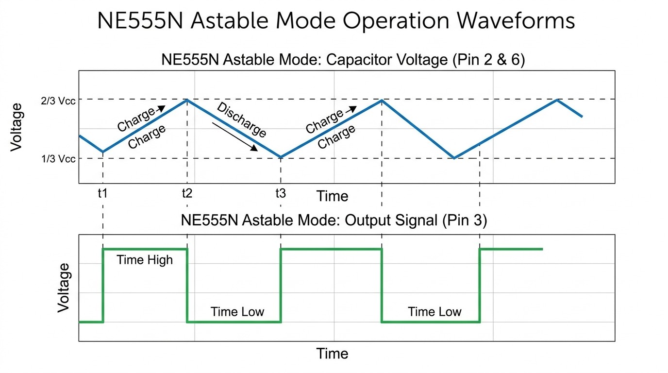
In real-time waveform behavior tests, an oscilloscope overlay demonstrates the exact relationship between the capacitor's charge/discharge curve (a blue sawtooth wave) and the output pulses (a green square wave). Visual evidence proves that the "high" output signal stays active only while the capacitor is charging from the 1/3 Vcc threshold to the 2/3 Vcc threshold.
Monostable Mode (One-Shot Timer)
Monostable mode generates a single, precisely timed output pulse when Pin 2 receives a low-voltage trigger.
The formula for the pulse duration is:
Time (T): 1.1 × R × C
The 1.1 constant is derived from ln(3), representing the time required for the capacitor to charge from 0V to 2/3 Vcc. For practical implementation examples of this mode, review A brief Analysis of the 555 Timer Circuit and its Project Applications.
Bistable Mode (RS Flip-Flop Bypass)
In Bistable mode, the external timing RC network is discarded entirely. The user leverages the IC's raw internal flip-flop, effectively turning the precision timer into a basic memory cell or toggle switch controlled by the Trigger and Reset pins.
Engineers note that digital simulators often "bug out" or fail to render this specific configuration accurately. Consequently, physical breadboard testing is required to verify Bistable operation.
Hardware Timers vs. Microcontrollers
Hardware timers like the NE555N operate directly at higher voltages and free up microcontroller resources by handling continuous pulse generation independently.
When to Use the NE555N Over an MCU
Modern microcontrollers (MCUs) like the Arduino or PIC series are the industry standard for complex logic and variable Pulse Width Modulation (PWM). For users who need software-defined timing changes based on sensor data, an MCU remains the stronger choice.
However, for engineers who prioritize simplicity and direct high-voltage operation, the NE555N offers a more robust path. The NE555N operates directly at up to 16V, eliminating the need for a 5V step-down regulator required by most MCUs. Furthermore, utilizing a hardware timer prevents the waste of valuable MCU pins on simple oscillation tasks. For more on resource management, see this VFD Driving Guide: What to Do When Your MCU Runs Out of Pins.
Common Wiring Mistakes and Troubleshooting
Most NE555N circuit failures stem from floating pins, lack of decoupling capacitors, or exceeding the 200mA output current limit.
Pin 4 Reset Configuration and Floating States
A common consensus among enthusiasts on community forums is the frustration of an output that refuses to switch or remains stuck high. This is almost always caused by a floating Reset pin.
Pin 4 must be tied to Vcc for normal operation. If left disconnected, ambient electromagnetic noise will induce voltages that constantly trigger the reset state. As highlighted in recent video intelligence regarding breadboard prototyping: "We almost forgot to pull up the reset to Vcc... that would be an issue because the IC would be in a reset state constantly, so the LED wouldn't light up."
Pin 5 Noise Filtering and False Triggering
Users frequently report inaccurate timing or false triggering when operating the NE555N near noisy power supplies. While many basic tutorials ignore Pin 5 (Control Voltage), professional workflows require grounding this pin through a 10nF (0.01µF) ceramic capacitor. This specific component stabilizes the internal comparator thresholds against electromagnetic interference, ensuring the 1/3 and 2/3 Vcc reference points do not fluctuate.
Power Supply Decoupling and Thermal Management
If the NE555N is getting hot during operation, the user is likely exceeding the 200mA sink/source limit or experiencing high-frequency oscillation due to power rail instability.
To prevent erratic behavior, a 10µF bypass capacitor must be placed across the Vcc and Ground rails as close to the IC as possible. Without this decoupling capacitor, the high-speed switching inside the bipolar NE555N causes sudden current draws, creating voltage spikes that destabilize the entire circuit.
Closing Summary and Next Steps
The NE555N remains a highly relevant, robust timing IC for modern hardware design. While microcontrollers dominate complex logic, the NE555N provides reliable, high-voltage pulse generation without writing a single line of code. Success with this component requires strict adherence to datasheet limits—specifically the 16V maximum operating voltage and 200mA current limit—alongside proper noise filtering on Pins 4 and 5.
To master this component, calculate a basic RC timing network using the Astable formulas provided above, and construct an LED flasher circuit on a physical breadboard to observe the hardware timing principles in action.
Frequently Asked Questions
What is the specific meaning of the "N" suffix in NE555N?
The "N" suffix designates a Plastic Dual In-Line Package (PDIP-8). It is functionally identical to the "P" suffix; the difference simply indicates the manufacturer (STMicroelectronics/ON Semi uses "N", while Texas Instruments uses "P").
What happens if I leave the control voltage pin (Pin 5) unconnected?
Leaving Pin 5 floating makes the internal voltage divider susceptible to electrical noise. This causes the 1/3 and 2/3 Vcc thresholds to fluctuate, resulting in false triggering and inaccurate timing. Always bypass Pin 5 to ground with a 10nF capacitor.
Can I use the NE555N in a modern 3.3V logic circuit?
No. The bipolar NE555N requires a minimum operating voltage of 4.5V. For 3.3V logic circuits, you must use a CMOS variant like the ICM7555 or TLC555, which operate down to 2.0V.
How do I protect the NE555N from inductive voltage spikes when driving a relay?
When driving an inductive load like a relay coil from Pin 3, you must place a flyback diode (such as a 1N4007) in reverse parallel across the relay coil. This provides a safe path for the high-voltage spike generated when the magnetic field collapses, preventing it from destroying the NE555N's output stage.
What is the maximum frequency the NE555N can reliably generate?
While the bipolar NE555 datasheet states a theoretical maximum operating frequency of 500 kHz, practical and reliable operation is typically limited to around 100 kHz. This limitation is due to internal propagation delays and the discharge transistor's sink current limits. For applications requiring frequencies above 100 kHz, CMOS variants or dedicated crystal oscillators are required.
 UTMEL
UTMEL
We are the professional distributor of electronic components, providing a large variety of products to save you a lot of time, effort, and cost with our efficient self-customized service. careful order preparation fast delivery service
 Discovering New and Advanced Methodology for Determining the Dynamic Characterization of Wide Bandgap DevicesSaumitra Jagdale15 March 20242881
For a long era, silicon has stood out as the primary material for fabricating electronic devices due to its affordability, moderate efficiency, and performance capabilities. Despite its widespread use, silicon faces several limitations that render it unsuitable for applications involving high power and elevated temperatures. As technological advancements continue and the industry demands enhanced efficiency from devices, these limitations become increasingly vivid. In the quest for electronic devices that are more potent, efficient, and compact, wide bandgap materials are emerging as a dominant player. Their superiority over silicon in crucial aspects such as efficiency, higher junction temperatures, power density, thinner drift regions, and faster switching speeds positions them as the preferred materials for the future of power electronics.
Read More Applications of FPGAs in Artificial Intelligence: A Comprehensive GuideUTMEL29 August 20255596
This comprehensive guide explores FPGAs as powerful AI accelerators that offer distinct advantages over traditional GPUs and CPUs. FPGAs provide reconfigurable hardware that can be customized for specific AI workloads, delivering superior energy efficiency, ultra-low latency, and deterministic performance—particularly valuable for edge AI applications. While GPUs excel at parallel processing for training, FPGAs shine in inference tasks through their adaptability and power optimization. The document covers practical implementation challenges, including development complexity and resource constraints, while highlighting solutions like High-Level Synthesis tools and vendor-specific AI development suites from Intel and AMD/Xilinx. Real-world applications span telecommunications, healthcare, autonomous vehicles, and financial services, demonstrating FPGAs' versatility in mission-critical systems requiring real-time processing and minimal power consumption.
Read More The 2026 Engineer’s Guide: Choosing the Right MCU for Your Next IoT & New Energy ProjectUTMEL30 April 20261887
A comprehensive comparison of 2026's leading MCUs from ST, NXP, and Microchip across power efficiency, processing performance, connectivity, and ecosystems to help engineers select the optimal chip for next-gen IoT and new energy projects.
Read More AI Server Components: Engineering Next-Gen Data Center Hardware for 100kW RacksUTMEL15 May 20261009
The transition from traditional enterprise IT to AI-driven workloads has rendered legacy data center hardware obsolete, forcing infrastructure planners to re-engineer server components for extreme thermal environments.
Read More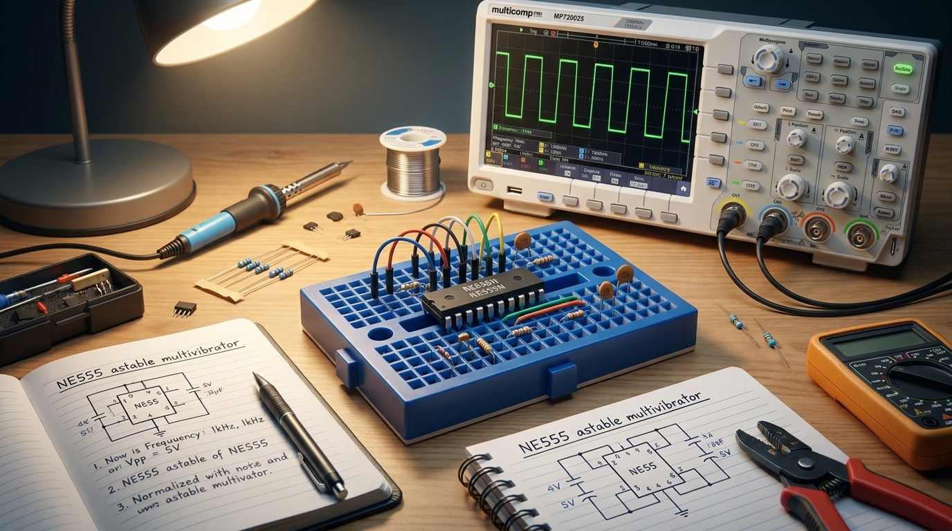 The Practical Engineer’s Guide to the NE555N Timer: Pinout, Setup, and TroubleshootingUTMEL29 May 2026807
This comprehensive guide explores the NE555N timer, detailing its 8-pin layout, internal architecture, and key datasheet specifications. It compares the bipolar IC to CMOS variants and details setup configurations for astable, monostable, and bistable modes. Additionally, the guide offers practical troubleshooting advice to prevent common breadboard failures, such as floating reset pins and electrical noise issues.
Read More
Subscribe to Utmel !
![MCP2036-I/P]() MCP2036-I/P
MCP2036-I/PMicrochip Technology
![ATAES132A-MAHEQ-T]() ATAES132A-MAHEQ-T
ATAES132A-MAHEQ-TMicrochip Technology
![ATECC508A-SSHCZ-B]() ATECC508A-SSHCZ-B
ATECC508A-SSHCZ-BMicrochip Technology
![HCS360-I/P]() HCS360-I/P
HCS360-I/PMicrochip Technology
![HCS361-I/SN]() HCS361-I/SN
HCS361-I/SNMicrochip Technology
![ACPL-W341-500E]() ACPL-W341-500E
ACPL-W341-500EBroadcom Limited
![UCC21520DW]() UCC21520DW
UCC21520DWTexas Instruments
![ADUM3220ARZ]() ADUM3220ARZ
ADUM3220ARZAnalog Devices Inc.
![HCS515-I/P]() HCS515-I/P
HCS515-I/PMicrochip Technology
![ACPL-W340-500E]() ACPL-W340-500E
ACPL-W340-500EBroadcom Limited


